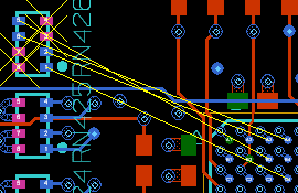
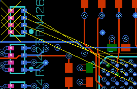
In order to have a clean route, occasionally the designer may have to swap pins or gates on some devices. Usually the devices that require pin or gate swaps include resistor networks, capacitor networks, gated ICs (such as buffers), inverters, analog gates, and occasionally FPGAs.
In every case the designer must consult with the engineer and get permission to make any changes. After making any changes, the information must be fed back to the engineer in the form of a was/islist or back annotation directly to the schematic.
Pin Swapping
Pin swapping is when the individual pins of a single device are swapped. Typically this is done on resistor networks. Figure 53 is an example of swapping pins 4 and 5, and pins 3 and 6.
Before Pin Swap
After Pin Swap
Gate Swap
Unlike pin swapping, which is the swapping of individual like pins (e.g., bi- directional or I/O pins) within the same package, gate swapping is the swapping of one or more pins (combination of input, output, etc. pins that make up a circuit) within the same package or another package that is of the same part number. When gate swapping, be sure to consult the datasheet of the part number to ensure that the gates of a device are indeed compatible, and to verify how the device is pinned out.
The following images illustrate a resistor network being gate swapped within the same package. The four gates in this case are pins 1 and 8, 2 and 7, 3 and 6, and 4 and 5.
Before Gate Swap (Within Package)
After Gate Swap (Within Package)
The following images illustrate a resistor network being gate swapped between packages (RN414 and RN415).
Before Gate Swap (Between Packages)
After Gate Swap (Between Packages)


.png)
.png)
.png)
-1.png)


![Download Optimum's Designer Handbook! [PDF format]](https://no-cache.hubspot.com/cta/default/317720/240d1413-c945-4cb8-a546-a84937b16039.png)