18.01.2018
Transmission Lines in RF PCB Design

Transmission Line Fundamentals
Over the last ten to twenty years, advances in IC fabrication technology have led to huge increases in both the operating frequencies and edge rates of switching signals in digital circuits. This has really pushed digital circuit design into the frequency domains that were previously considered RF and/or microwave. As a result, it has become important to consider the transmission line parameters of the connecting traces used for digital signals in circuit boards as much as they have always been considered for RF connections.
A transmission line is a two or more port network connecting a generator circuit at the driving end to a load at the receiving end. Transmission lines most commonly consist of two conductors (although sometimes more). A three phase power transmission line for example uses three or more conductors. Examples of commonly used transmission lines are a simple two-wire line, a co-axial cable, or a circuit board trace and return path as in the case of microstrip and stripline.
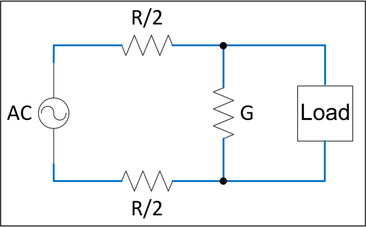
At DC and low frequencies, where wavelength is much longer than the circuit path, a transmission line was often thought of in terms of resistance only and early transmission line modeling was based on resistive loss with voltage drop as the only real concern. Analysis could be done using traditional static circuit theory and lumped elements. An equivalent electrical circuit used for DC analysis of low speed transmission lines could be created with resistive elements only, as follows:

Figure 1. Resistive Model Of A DC Or Low Speed Transmission Line
The voltage drop in each conductor is calculated using only the resistance, R, of the line and the current flowing in the line. The larger the cross sectional area of the conductor, and the higher the conductivity of the material, the lower the resistance. The conductance, G, represents the leakage current through the dielectric material between the two conductors, at DC and low frequencies this can be dismissed as negligible.
At higher frequencies however, the wavelength is now much shorter than the typical circuit size, the parasitic inductive and capacitive elements of the transmission line start to have an effect and the behavior of the transmission line is considerably different. Analysis requires high frequency transmission line theory with distributed elements.
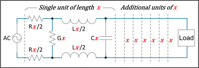
An equivalent electrical circuit for a high speed transmission line can be drawn with only passive components in a ladder network. The complete transmission line is made of cascaded sections of the same equivalent circuit. For exact analysis we would need an infinite number of infinitely small segments of length x. The transmission line can then be represented as follows:

Figure 2. Complete Model Of A High Speed Transmission Line Showing Parasitic Elements
If we assume the transmission line is physically constant and the dielectric is uniform over the entire length, then usable results can be modeled by defining the characteristics of the transmission line per unit length.
There are four primary transmission line parameters, as follows:
- Capacitance per unit length, Cx, given in Farads, is the capacitance between the two conductors over the length x. The capacitance is a function of physical dimensions of the conductors, the separation between the conductors and the dielectric material between them.
- Resistance per unit length, Rx, given in Ohms, is the loop resistance of the pair of conductors over the length x. The resistance is a function of the physical dimensions and material properties of the conductors.
- Inductance per unit length, Lx, given in Henrys, is the loop inductance of the pair of conductors over the length x. The inductance is a function of the physical dimensions and the separation of the conductors.
- Conductance per unit length, Gx, given in Siemens, is the conductance between the two conductors over the length x. The conductance is a function of the losses of the dielectric between the conductors.
There is a wealth of information regarding the analysis of transmission line characteristics and the effect these characteristics have on high frequency signals. It is important that layout designers understand that the traces they create in their designs are not simply copper connections to transfer a signal from one point to another, albeit that is what they actually do. These connections are actually transmission lines, and need to be designed carefully if they are not to cause the design to function poorly or even not at all.
The higher the operating frequencies, and more importantly, the faster the edge rates of the signals, the more important it is to understand that transmission line design needs to be considered. Higher signal speeds and edge rates means that what used to be considered a short trace is now actually a long trace in terms of the wavelength of the signal.
Fortunately, there are also many advances in both device technology and fabrication processes that actually work in the layout designer’s favor when designing circuit boards for these high frequencies. Traces and spaces can be much smaller than was previously the case, dielectrics are much thinner and of higher quality materials, and components are becoming much smaller which allows us to place them closer together. These factors all work to allow us to create complex, high density, high speed designs where the transmission length of the signals can be much shorter than was previously the case.
Detailed transmission line analysis is an extremely complex topic, and is well beyond the scope of this guideline. In the next sections some common types of planar transmission lines used in circuit board design are shown and the formulae for calculating the characteristic impedance and propagation delay. This is by no means a complete reference on any of these transmission line structures. One of the most complete references available, and highly recommend to both layout designers and electrical engineers, is:
Transmission Line Design Handbook
Brian C. Wadell
Artech House, 1991
ISBN 0-89006-436-9
This post is a condensed snippet from A Practical Guide to RF and Mixed Technology Printed Circuit Board Layout, written by Optimum's Brendon Parise. Available for purchase by following this link.


