PCB DESIGN LAYOUT
Our world-class electronic design team is uniquely qualified to handle your toughest challenges
We can’t be beaten on quality, consistency, and on-time delivery
Sure, every design team has experience. But our experience spans 10,000 design projects over 30+ years for hundreds of companies. At Optimum, we like to say we’ve seen it all, and if we haven’t, we love to be challenged by the latest cutting-edge technology and circuit board design techniques.
We employ elite designers
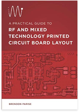
We’re RF and Mixed Signal experts; in fact, we wrote the book on it. Manufacturability is part of our DNA. Whether your primary concern is cost or reliability, our designers are strong collaborators and advisers and always focused on achieving the desired results.
We are power users of today’s EDA software tools
All of our designers are multi-tool disciplined and follow a rules-driven approach. We embed all topology, timing, and manufacturing rules into each of the tools we use.
We pay attention to the details
Although we encourage creativity, our processes ensure each design carries the highest Optimum signature standards to safeguard consistency no matter the project. Our processes are documented, knowledge is shared through our Wiki intranet, and checklists are utilized as a part of our ISO certification. Additionally, every design is run through a stringent Valor DFM analysis to help ensure a smooth transition into manufacturing.
We always have time for you
Our business model ensures we are never more than 80% of capacity. You’ll receive the attention and resources needed for a successful delivery when you work with us. This relentless, proactive project management approach ensures we’re marching to your vital schedule demands.


