31.03.2014
Clearance and Creepage Rules for PCB Assembly
Electrical spacing rules become significant from a product safety perspective when the normal operating voltage is greater than 30VAC or 60VDC. It may come as a surprise that voltages above these levels are considered hazardous and that these designs are therefore considered high voltage.
Having designed a number of high voltage and mixed technology boards recently, I have had to research current standards, definitions, and methodologies used to implement high voltage spacing rules in confined spaces. I say spacing rules because, in addition to the normally-supplied “clearance rules,” there is another set of spacing rules that are just as important to follow for high voltage designs—namely, “creepage” rules.
The following discussion defines these spacing rules, both clearance and creepage, and suggests some methodologies to help ensure that the rules are correctly applied and adhered to.
Design Trends
Increasingly in printed circuit board (PCB) design we are driven to reduce size and increase component density on circuit boards in the quest for miniaturization and reduced costs. This mindset is not confined to handheld products; it has become prevalent across the entire electronics product development industry. Newer high-density components make this a possibility. There are times, however, where this miniaturization presents some significant challenges to the designer, particularly with mixed technology where high voltage circuits are part of the design. Some examples are solar energy conversion and handheld medical imaging products. In the past, it was common to design high voltage boards as a separate piece in a multi-board system. Now, the continuing drive towards miniaturization means that we don’t have space for multiple boards, and there is an increase in the number of designs utilizing mixed technologies where analog, digital, and RF circuits are closely combined with high voltage circuits. These high voltage circuits require additional rules in the form of increased electrical clearances and isolation for operator safety. We need to be aware of these rules and find ways to implement them while still reducing overall product size.
Clearance vs. Creepage
Engineers usually provide the spacing rules for a design in the form of a table or list, invariably titled “Clearance Rules.” And virtually all PCB design software tools refer to all spacing rules as clearance rules. This is not technically correct, and this becomes an important distinction to make in high voltage designs. The parameters for pad-to-pad, pad-to-trace, trace-to-trace spacing—basically any spacing rule that is applied between conductive elements over an insulating surface—is creepage, not clearance. Spacing between conductive elements through air is clearance. The general term ‘clearance rules' will undoubtedly continue to be used for specifying all spacings, both by engineers and design software developers, so designers need to be aware of the difference between creepage and clearance, and always make sure they have both sets of rules when the design is considered high voltage.
Another item to note is that creepage requirements are always greater than or equal to the associated clearance requirement. It is quite easy to satisfy either a creepage or clearance rule between two electrical nodes and at the same time have a violation in the other rule, so extreme care must be taken during all phases of PCB design to ensure that both rules are always satisfied.
Definitions per IEC60950 standard:
Although we have defined creepage and clearance informally, the IEC standard has more precise definitions:
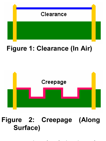
CLEARANCE: The shortest path between two conductive parts, or between a conductive part and the bounding surface of the equipment, measured through air (Figure 1).
CREEPAGE: The shortest path between two conductive parts, or between a conductive part and the bounding surface of the equipment, measured along the surface of the insulation (Figure 2).
One additional term that is related to these definitions in a high voltage design is “bounding surface.”
BOUNDING SURFACE: The outer surface of an electrical enclosure, considered as though metal foil were pressed into contact with accessible surfaces of insulating equipment. An example is a metal enclosure that the PCB is mounted into.
Other factors:
Combinations of pollution degrees and insulation types are some other factors to keep in mind when considering the clearance and creepage requirements of a given design. The pollution degree is generally what the name implies; that is, the amount of dust, moisture, and other particulate matter in the air surrounding, or on the surface between, high voltage nodes. Some of the insulation types are termed functional, basic, double, supplementary, and reinforced. These insulation definitions can be quite complex. There are multiple standards with different definitions of both these parameters, so the appropriate standard(s) for the design in question should always be referenced prior to commencing the design in order to be certain that all rules are known and applied.
So what do we need to do?
The problem we have is that while PCB real estate continues to shrink as we make products smaller and smaller, we also have to still be able to meet both clearance and creepage rules for high voltage designs. So we need to have some strategies available for us to implement the required spacing, but do it with less overall space available to us. Even though clearance is generally less than creepage, it can often be the more difficult rule to satisfy. The following is a discussion of some of the strategies that can be used.
Solving clearance issues:
Clearance is measured in air (line of sight), so there is little that can be done at the layout level to reduce the required spacing. Careful placement does make a difference, but the more significant reductions in spacing can be achieved by using insulating materials and, when possible, by double-sided assembly. Insulating materials can be a sheet barrier between high voltage nodes, or sleeving overexposed high voltage leads. Since a high proportion of parts are surface-mounted, it is possible to place circuits requiring clearance on opposite sides of the board. Remember to maintain clearance from the bounding surface and through-hole connection points, if present. Nodes within the same high voltage circuits at the same potential usually do not require increased clearance or creepage to each other, but do require clearance to low voltage circuits. A good method is to place high voltage circuitry on the top side of a board and low voltage circuits, often control and monitoring, on the bottom side. This usually works fine because often there is less space between the bottom side of a board and the chassis, and the low voltage circuitry usually does not have the clearance requirement to the bounding surface (housing) that high voltage circuitry does. While some standards allow the use of conformal coating to reduce the clearance requirement, others do not. So it is important to make sure you consult the relevant standards for your design.
Solving creepage issues:
As we know, creepage is the spacing between electrical nodes over an insulating surface. In our discussion this means the space between conductors on the surface or internal layers of a PCB. Simply spreading out parts further is not going to meet the packaging needs so here are some strategies that will allow higher packing density while helping to meet the required creepage distance.
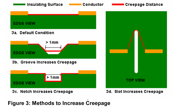
Figure 3 shows various scenarios for potentially increasing creepage distances. The normal condition on a flat surface is shown in Fig. 3a. Creepage is measured over the surface between the nodes.
In Fig. 3b, a V-groove can increase the surface distance between the nodes. The increased length is only measured down the groove to the point where it reduces to 1mm width.
A parallel-sided notch (Fig. 3c) can increase the surface distance further, but must be 1mm or greater in width. A notch such as this can be more costly than a groove to implement.
Finally, a slot of greater than 1mm width can be used to increase the surface distance further again (Fig. 3d). This is the easiest method to increase creepage and also probably the most cost-effective. It does, however, require considerable free space in one direction, so it may not always apply.
Examples:
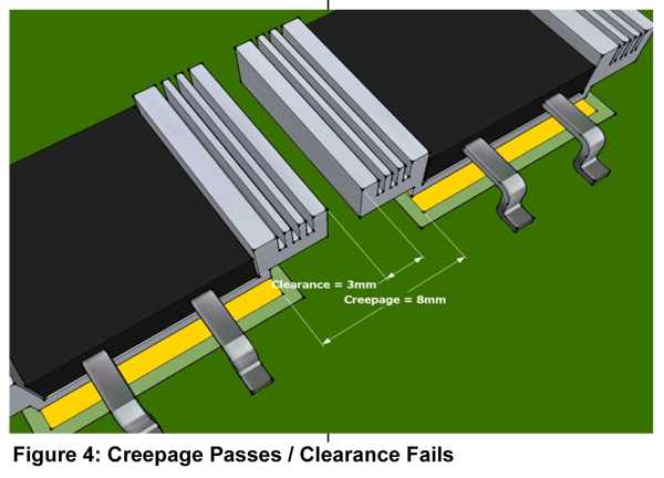
Consider a circuit where the clearance and creepage requirements are defined as 4mm and 7mm, respectively. Now look at the designs in Figures 4 and 5. The DPAK devices mounted on heatsinks in Figure 4 will pass the creepage requirement because the surface distance between the DPACK pads is 8mm, but this design will fail clearance because the heatsinks are too close together, at 3mm. The only effective fix for this is either moving them further apart if the space exists, or finding a different placement altogether.

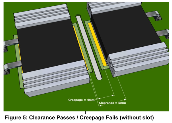
In Figure 5 the same devices are placed differently and the clearance requirement is satisfied, at 5mm, but now creepage will fail at only 4mm. If circuitry on all layers allows, this can be easily fixed by placing a slot, as shown, between the two DPACK pads that extends at least 1.5mm beyond the length of the pads (in this case it would be less than the extents of the heatsink, so it should be possible). The creepage distance, instead of simply straight-line pad-to-pad distance, is now measured between the corners of the DPACK pads, but must now go around the slot, which gives a much higher creepage value, and the design will pass.
What are the standards?
There are numerous standards that attempt to define clearance and creepage requirements for PCB design. Probably the best known are IPC2221A and UL60950-1. These and other standards provide quite different rules and the required rules are also significantly affected by different environmental factors. Providing definitive rules is beyond the scope of this short article, and designers should consult the relevant standards depending on the end use and the typical operating environment of the product.
Clearance tables in these standards, based on peak and DC operating voltages, provide safe isolation distances to be applied on the PCB. Of note, though, is the IPC2221A table which, in general, provides isolation distances that are typically in excess of the minimum requirement. If a design is done according to the IPC2221A rule set, then it can be safely assumed that adequate isolation has been provided. The UL60950-1 standard provides much more detail in terms of pollution degrees, insulation types and required isolation distances. The standard to be applied depends on the required test standards the end product is to conform to. Careful examination of the rules and environmental factors becomes more important when the design is compressed to a degree where the more generous rules cannot be applied.
References:
The following is a list of some relevant standards for PCB design creepage and clearance requirements:
IPC2221A: Generic Standard on Printed Board Design.
UL61010-1: Electrical Equipment for Laboratory Use.
UL60950-1: Safety of Information Technology Equipment


![Download Optimum's Designer Handbook! [PDF format]](https://no-cache.hubspot.com/cta/default/317720/240d1413-c945-4cb8-a546-a84937b16039.png)