31.03.2014
DDR Memory Layout Design: Rules, Factors, Considerations

Jump rope is a popular childhood activity involving two people swinging the ends of a long rope, with a third person in the middle skipping each time the rope swings under their feet. Now, imagine those same two people swinging not one rope, but two ropes in opposite directions, with the person in the middle working twice as hard. This is “double Dutch” jump rope, and it takes a much higher degree of skill than jumping a single rope because for each cycle of swings, there are two ropes to coordinate rather than just one. And if more than one jumper is in the middle skipping the ropes, the degree of difficulty skyrockets!
Many of today’s printed circuit board (PCB) layouts use some form of Double-Data Rate (DDR) memory, which is like going from a single jump rope to double Dutch. DDR allows two data bit transitions to occur during a single clock cycle, instead of a single data bit transition—as previously in Single Data Rate (SDR) memory—effectively doubling its data throughput. The increased speed of these memory circuits has made the complexity of the PCB layout more demanding with respect to bus timing and signal integrity and, as a result, designers employ a prescribed set of layout techniques in order to meet these demands.
Important PCB Layout Factors in a DDR Design
Memory circuits have typically had to meet certain requirements in their layout in order to function properly. This was true of SDR memory, and it is true of DDR memory as well. However, the doubling of data throughput in DDR using two transitions in one clock cycle has tightened the requirements, making the necessity more acute. These requirements include the following:
- Proper Setup/Hold Time
- Clean Supply Voltages
- Proper Termination
- Trace Length Matching
- Optimum Operating Temperature
We will look at each of these factors in turn, and discuss the methods used to achieve them in the PCB design.
Proper Setup/Hold Time
Most double Dutch players like to jump into and jump out of the ropes many times during a session, with many players inventing creative and elaborate approaches. Their timing must be just right, or else one of the ropes will catch them on their shoulder or foot, breaking the rhythm and bringing the game to a halt. The player needs to have time to set up their entrance or exit so that everything runs smoothly. And if two or more players are going to make the transition, it is all the more important that they be ready at the same time.
The DDR Clock (CLK) lines determine the timing of data input and output to and from the memory chip. They are the heartbeat of these devices. They set the window of time in which the data must be ready to be accepted or ready to be extracted (jumping in or jumping out). Each bit of the data bus must arrive and stabilize before the clock cycle. This is called setup time. The entire bus must also remain steady while being read in or out after the clock. This is called hold time. Since DDR devices require this prescribed amount of setup and hold time, it is critical that the clock be designed to arrive at just the right instant.
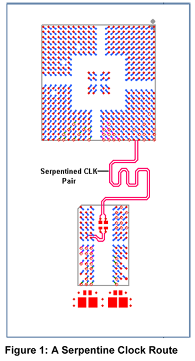
Since we cannot speed up electrical impulses (they can only ever travel at the speed of light), the way to adjust the speed of arrival is to add delays between the source and destination by increasing trace length using a serpentine routing strategy.
Figure 1 shows a clock circuit for a DDR device. The clock is a differential pair, of which the source and destination are too close for the timing involved. The differential pair has had length added to the routing in the form of bends, so that it takes longer to arrive at its destination. Obviously, this takes up more space on the PCB, making the design process more difficult. And in order to route the clock signal properly, the design tool must also include a method of specifying the timing requirement and letting the designer know when that requirement has been met when adding length to the traces.

Improper clock timing would be catastrophic, causing massive data corruption and bit errors. These timing errors would need to be analyzed using the proper scoping equipment and timing analysis, making the debug cycle of the PCB ever more intricate.
Clean Supply Voltages
DDR design requires as clean a power supply and reference voltages as possible. This is analogous to having a steady and flat surface on which to play double Dutch. Variations of voltage (like variations of surface height) may cause unpredictable results. Depending on the type of DDR, reference voltages and termination references will play very critical roles in determining overall signal integrity (SI) and data bit registration (that is, whether the device determines the signal to be a One or Zero). Reference voltages that are not set to correct levels or that are improperly filtered may cause the referencing signals never to trigger or to trigger prematurely. Any design that utilizes termination schemes requires that its termination be stabilized properly with bypass capacitors, aiding in the bus signal integrity. Bus signals that are not properly terminated can exhibit SI issues, which could cause false triggering.
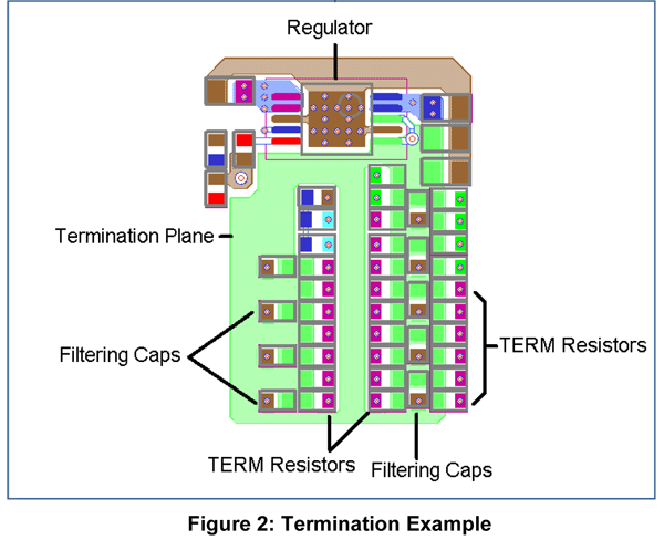
Figure 2 is an example DDR Address/Command (ADDR/CMD) termination circuit. Proper, clean voltage for the termination resistors is very critical. In this example, the supply voltage is delivered through the plane from the regulator IC to the termination resistor elements on the same side of the board, thus eliminating the impedance that vias add. Capacitors are also evenly placed, which creates a consistent, clean bypassed reference.

Trace Length Matching
When designing a PCB that contains DDR circuits, it is very important to also consider and account for trace length matching. Routed buses will only operate correctly if very tight timing margins are properly maintained. These margins are created on the PCB by adding specified delay lengths. These length constraints are usually very well documented in manufacturers’ datasheets. DDR buses will be broken into group classes and routed in a specific sequence, in order to facilitate proper timing, as the timing relationships between the groups must be observed.
Common length matching route groups are:
- Clock-to-Address/Command Group
- Clock-to-Strobes Group
- Strobe-to-Data Group
Clock-to-Address/Command Group:
The purpose of the Clock-to-Address/Command Group (abbreviated CLK/ADDR/CMD) is to match the overall length of the CLK signal(s) to all ADDR and CMD signals specified. Depending on memory type, density, and bank structure, this group can get complicated, as there may be a complex signal topology scheme, which must be followed.
Clock-to-Strobes Group (CLK/STB):
The requirement for the CLK/STB group is to match the overall total length of the CLK signal(s) to the Strobe and Data. This required group matching ties the CLK timing to the Data timing. The allowable matching tolerance is usually defined in the manufacturer’s data sheet.
Strobe-to-Data Group (STB/Data):
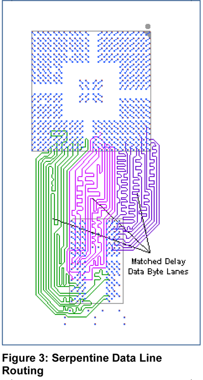
The final group—STB/Data—should match the STB signal(s) to the individual Data bit signals. Since the number of signals that a Data group can contain may be large, the Data group is generally broken into “Data Byte Lanes.” Each lane contains eight Data bits, plus one Data mask, and one STB, and all signals in this group must be length matched to specification.
Figure 3 shows typical byte lane matching. The matching requirement for the individual Data bits is only relevant within each byte lane. Three separate colors represent the individual byte lanes, showing that each lane is not required to be the same exact routed length as the other lanes. Overall data timing is maintained by keeping the STB in each byte lane within timing tolerance relative to CLK. Once again, the allowable tolerance is usually defined in the manufacturer’s data sheet.

Time of Flight: One more length matching consideration is Total Time of Flight. With DDR timing margins decreasing, it is becoming more important to also consider a signal’s total Time-of-Flight (TOF). The TOF value is the total of both PCB trace length plus any additional length inside part packages. It is imperative to know the package length information, and to add this length to your total “overall” signal path length when calculating matching.
If Signal bus delays are not properly timed by lengthening the appropriate PCB copper, then improper signal timing will result.
Optimum Operating Temperature
Most of us would not be able to jump rope very long in 105° temperature or higher, nor in temperatures below 40°, even if we were practiced and in good shape. DDR circuits are also affected by temperature, altering their performance. As with any design, temperatures can affect performance. Part efficiency with increased or decreased temperature can cause timing margins to drift, making it essential to account for any possible timing drift in the design process. Generally, chip manufacturers’ guidelines will contain recommended tolerance margins.
What happens if proper design practices are ignored?
Failure to follow the above design parameters will produce circuits that do not perform as intended and will function erratically. Often the circuits can malfunction so minutely that data corruption can be seen at only specific operating temperatures or when particular data streams are passed in and out of the memory chips. At other times the failures can be seen as data corruption. In any case, improperly functioning circuits can be very difficult to troubleshoot. Many times on non-FPGA controller designs (ASIC designs that do not have the ability to individually adjust signal timing parameters) it will not be possible to correct the timing errors without re-layout of the copper on the PCB.
Design It Right!
Considering all the critical elements of several players playing double-Dutch jump rope, it is crucial that everyone know their part in keeping the rhythm going, and to time their movements precisely. Otherwise, someone is in the wrong place at the wrong time, and the ropes stop turning, bringing the entire game to a crashing halt.
And considering all the critical elements that are required when designing DDR circuits, it is crucial that an experienced PCB designer who can understand, interpret, and execute a design that meets specific, critical timing conditions is required. This task should be accomplished with proper analysis of the specified parts’ data sheets, white papers, and application notes. Proper use of a design layout constraint manager will also prove extremely valuable in reducing design cycles while maintaining proper signal integrity.


![Download Optimum's Designer Handbook! [PDF format]](/hs-fs/hub/317720/hub_generated/resized/3f81ff4e-f8cf-4a7b-8bfb-a62958faa41a.png)