31.03.2014
HDI Layer Stackups for Large Dense PCBs
A few days into a recent project for one of our customers, the lead engineer called me to tell me that the PCB design would have to change…drastically! The design as originally conceived did not seem too difficult—a 20-layer board having active components on one side only, 2.75″ x 4.0″ in size, 284 parts with 2500 pins. That works out to about 228 pins/sq. in. The new requirement was to reduce the board size by 50%. Accomplishing this would prove to be much more difficult, and would require a complete rethinking of the strategies to get the board designed, eventually requiring the use of high-density interconnect (HDI) techniques. What follows is a description of some of the critical design decisions that had to be made along the way toward achieving success in the design effort.
Shrinking the Board
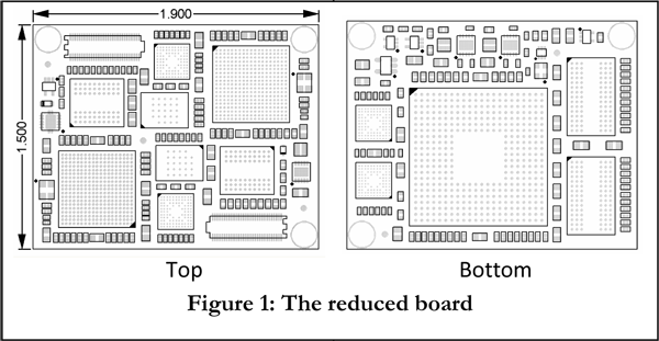
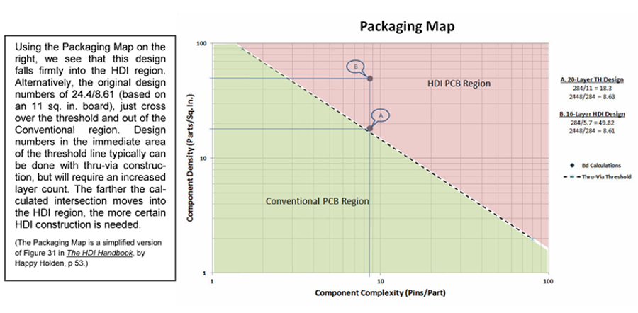
Working with the lead engineer, the first task was to remove all non-essential circuits. After whittling the schematic down to its bare bones and allowing active components to be placed on both sides of the board, we arrived at a final board size of 1.5″ x 1.9″ (2.85″ sq. per side, or 5.7″ sq. total area). This smaller form factor (Fig. 1) resulted in over 900 component pins per square inch of board space, a pin count that is considered very dense, based upon an available but underused, Packaging Map Formula[1]. The resulting pin count ended up well into the HDI region of this chart, so there was no doubt in anyone’s mind that this was going to be an HDI design.
Determining the Stack-Up
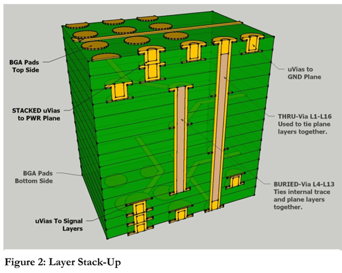
Only one component in the design required the use of micro-vias (μVia). That part is a .5mm pitch ball grid array (BGA). However, the entire design would require a much more involved HDI stack-up and fabrication to achieve full circuit connectivity. After numerous discussions with our customer and the board fabricator, we ultimately decided on a 16-layer, micro-via stack-up (See Fig. 2). This stack-up includes:
- The use of a 12/5 (.012”pad/.005” laser drill) stacked micro-vias.
- An 18/8 buried-via from layers 4-13.
- A 24/12 thru-hole-via from layers 1-16.
- Solid ground plane on layers 2, 5, 8, 11 & 15.
- Power planes on layer 3, 6, 9, 12 & 14.
- Buried capacitance materials for layer pairs 5/6, 8/9 and 11/12.
- Signal breakout traces on layers 1, 3, 4, 13, 14 & 16.
- Primary signal routing on layers 4, 7, 10 & 13.

With this stack-up, the PWR and GND pins—most of which are laser-drilled μVias—stop one or two layers deep into the board. This means that roughly 40% of the BGA pins’ break-out vias will no longer occupy internal trace routing channels. This frees up a large amount of routing space on the remaining internal layers, which enabled us to reduce the layer count from the original design.
The top-side BGA signal pins use μVias down to layers 3 and 4 (layers 14 and 15 for the bottom side) to break-out of the BGA areas for routing, as required. Using this stack-up’s combination of μVias, buried-vias, and thru-vias allows for back-to-back, high-pin-count BGAs and discrete components. The smaller HDI feature sizes offered enough improvement in the routing density to allow for full connectivity.
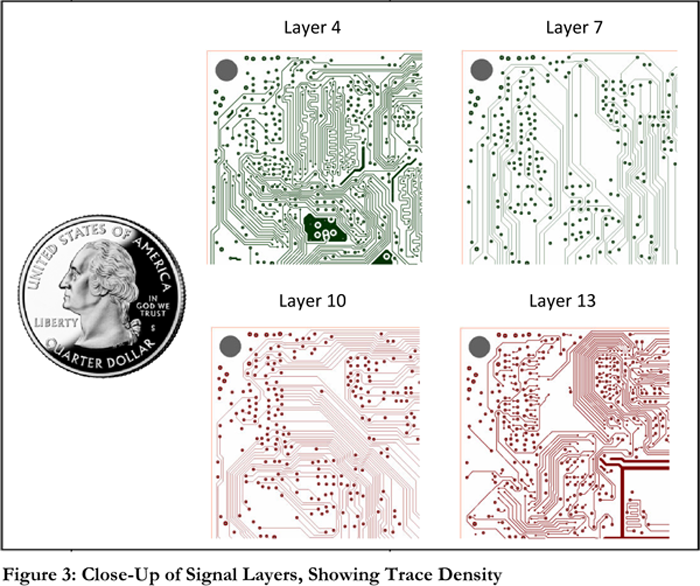
The illustrations in Fig. 3 show portions of the primary internal routing. Layers 2, 3, 14, & 15 are used primarily for break-out traces and planes, and have pads present for all μVias that either stop at that specific layer or continue on to layer 4 (layer 13 for the bottom side). Layers 4 and 13 have all three types of vias present and, combined with trace routing, give a good indication of just how dense the routing is. Layers 5–12 have only buried and thru vias, and have considerably more room for routing. The coin is shown to give an idea of just how small and dense these areas are.
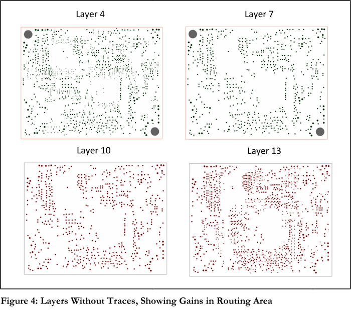
An expanded look at layers 4, 7, 10, and 13, without the traces (Fig. 4), gives an indication of the space that we gained for routing on the internal layers by using μVias. Layer 4 has 1,030 via locations, Layers 7–10 have 600 (a mix of buried and thru-vias), and Layer 13 has 1060. There are less than 40 thru-hole vias in the entire layout, and these are primarily used to tie the plane layers together.
By comparison, the original 20 layer, thru-via construction board required 8 internal routing layers in order to accommodate the wiring density, and would have resulted in a thicker board for the higher layer count.
IPC Standards -2226 and -2315 offer formulas for calculating component and wiring densities. These tools are useful for determining a starting point to begin discussions with your PCB designer and fabricator regarding the number of layers in the board stack-up.
Benefits Realized
Signal Integrity: One realized benefit of the HDI design for this project is the improvement in electrical performance. The smaller parts used here have shorter internal wire lengths, reduced rise times, and lower power requirements when compared to their larger, alternative packages. This HDI design extends the advantages of these smaller features. The μVias have considerably less electrical parasitic capacitance and inductance than thru-hole vias, partly due to significantly reduced stub lengths in critical circuits. They also have a large current-carrying capacity. Thin dielectrics between signal and plane layers were required to meet overall thickness and signal impedance targets, which help to keep trace widths small (<4mils). The solid copper power planes near the outer layers help reduce noise, as well as RFI/EMI emissions, in addition to opening up internal layers for more traces, as previously mentioned. The intentional use of buried capacitance plane layers reduces the number of bypass capacitors needed, by making the PCB itself work as a component. The effect of all of these characteristics works in combination to greatly improve the board’s overall signal integrity.
Additional Considerations
Customers should be aware of the prices and construction methods involved for HDI before deciding to use smaller pitch parts which require the use of HDI and μVias. As PCBs increase in complexity, cost increases range from 20% to 80%, depending upon the processes involved. The primary cost factors with HDI are due to the additional drilling, plating, and laminating processes and the materials used for plating and filling the μVias. The total number of μVias is fairly insignificant; the process is the same for just a few holes as it is for a large number of holes. Below are shown ballpark increases in cost for some of the additional processes.
Board Cost: My engineer’s original cost target was approximately $14 per board. Fab quotes for the original 20-layer design actually came closer to $18 per board. When we settled on the smaller form factor and the 16-layer stack-up, the per-board cost of the HDI design dropped to $15, a savings of about 17% from the original 20-layer estimate. This was primarily due to the increase in the number of boards per panel (twice as many as the larger original size), as well as the reduced layer count. Obviously, not all HDI designs are going to have such a positive cost impact. Although HDI is typically more expensive, it should not be assumed to always be so. With so many variables in play, all of the cost factors should be evaluated before a decision is made either for or against HDI.
Cost factors: (rules of thumb)
10-20 layers, add 10-20% per add’l layer pair
(above 20 layers costs climb even higher)
Non-conductive via fill +20%
Via-in-Pad, filled and planerized +25%
One-layer deep μVia -5%
As mentioned above, the fabrication process for HDI and μVia construction is more expensive than conventional thru-hole processing. Each successive μVia layer pair adds a lamination cycle to the construction process and, therefore, additional costs.
One Caveat
There is a downside to HDI construction. Due to having vias-in-pads (VIP) and the extremely small size of the parts and μVias, assembling the board, testing the circuits, and making any needed repairs are all the more challenging. The affected departments should be consulted, and methodologies must be created in order to provide solutions to their concerns.
Conclusion
HDI construction offers many opportunities for product design. By working with your designer and board fabricator and considering all of the various processes and methods for board construction available, cost-effective solutions can be found. By using the techniques of HDI in this design, our customer was able to meet the needs of two markets with one product, thereby increasing their profitability. The engineer with whom I worked called me a few weeks after the design was finished to let me know that they had finished testing, and were entering the production cycle.
When used appropriately, the end result of HDI design methods will be improved product performance, better price competitiveness, and new product innovation.


![Download Optimum's Designer Handbook! [PDF format]](https://no-cache.hubspot.com/cta/default/317720/240d1413-c945-4cb8-a546-a84937b16039.png)