23.04.2019
Embedded Microstrip Transmission Lines in RF PCB Design

Embedded Microstrip
Strictly speaking, the application of soldermask, conformal coating or other surface treatments will change a pure surface microstrip line to an ‘embedded or coated microstrip’ line. This, however, is not what is traditionally referred to as embedded microstrip line, and the determination of actual characteristic impedance is more difficult with these because of the inconsistency of dielectric constant and thickness of the material above the trace.
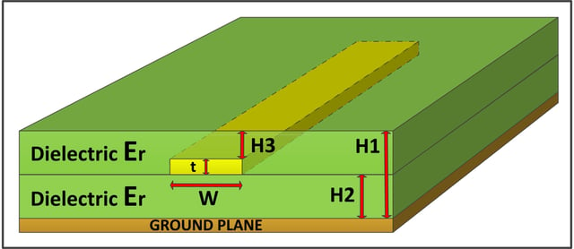
The type of line discussed here is actually what is known as ‘deeply embedded microstrip’ where, instead of air, soldermask or conformal coating, there is another layer of substrate material with a known thickness H3 and a known dielectric constant Er intentionally constructed above the trace.
Structure
An embedded microstrip transmission line, similar to microstrip, is made up of a conductor, usually copper, of width W and thickness t routed over a ground plane that is wider than the transmission line itself and separated by a dielectric substrate of thickness H2.
 Figure 1. Embedded Microstrip Transmission Line Construction
Advantages
- The trace will be better protected from exposure to the environment, this may be particularly useful in environments where there is a higher moisture content. This may also be relevant in harsh environments where solder mask alone may not provide adequate protection.
- The trace will be approximately 30% narrower than surface microstrip for the same characteristic impedance, depending on the thickness of the dielectric above the trace. This reduced trace width allows for a higher density of components and interconnects.
- The impedance is more easily defined and controlled because of the uniform dielectric constant above and below the trace. Surface microstrip impedance is more difficult to calculate and maintain.
- There may be a potential increase in surface layer placement sites since the trace is now internal to the board. This means the trace may be able to route under the body of some large components or connectors, depending on the signal being routed and the nature of the surface parts and circuits it is routed under. If the surface pads are very large though, be aware that the copper on the surface will change the characteristic impedance of the embedded microstrip trace for the portion of the trace that is under the surface layer pad.
- EMI radiation is slightly better than with surface microstrip, but the absence of a ground plane above the trace means that EMI with embedded microstrip is still a significant issue.
Disadvantages
- The board will be more difficult and more expensive to fabricate because multilayer lamination is required.
- For surface mount designs a via is needed to make the connection to layer 2, this adds resistance, capacitance, and inductance to the connection and these may be undesirable. The use of microvia in pad technology can offset the negative effect of a via to an extent because these vias are much smaller (lower capacitance), shorter (lower inductance) and are copper filled (lower resistance). Through hole designs can benefit from embedded microstrip because there is already a connection point available on all layers, so an additional via may not be required to connect to layer 2.
- Propagation speed is approximately 20% slower than surface microstrip. This is not very helpful when using a mix of surface and embedded microstrip and stripline for density, and the signals need to have matched delays. Differences in propagation delay of the transmission lines makes delay matching more difficult in most CAD systems because delays need to be matched in terms of time rather than the simpler matching in terms of length which is normally used when the propagation delays of the matched signals are the same.


![Download Optimum's Designer Handbook! [PDF format]](https://no-cache.hubspot.com/cta/default/317720/240d1413-c945-4cb8-a546-a84937b16039.png)