05.04.2019
Microstrip Transmission Lines in RF PCB Design

Microstrip is still by far the most commonly used transmission line structure in RF and microwave designs. This is becoming less the case though, as digital and mixed technology designs continue to increase in speed and density.
Because microstrip is typically a wider trace than stripline for the same impedance and because of the increased radiation associated with microstrip, it requires both more space to route and greater clearance to nearby traces. In a pure RF or microwave design this is not usually an issue, but with the demand for smaller product size and the resulting increased component density it is becoming an option not so easily afforded.
Structure
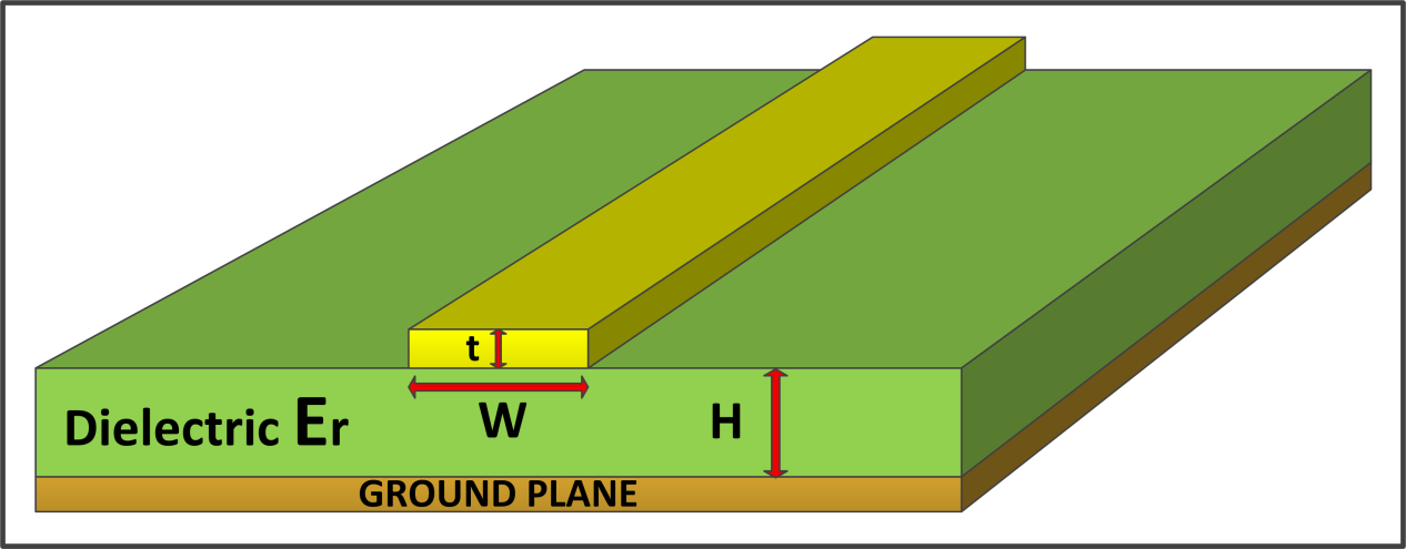
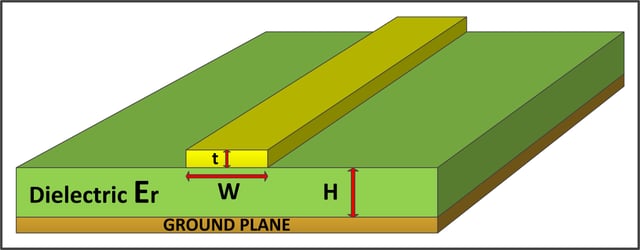
A microstrip transmission line is made up of a conductor, usually copper, of width W and thickness t routed over a ground plane that is wider than the transmission line itself and separated by a dielectric of thickness H. (See Figure 1 below). Best practice is to ensure the ground reference plane extends by a minimum of 3H on either side of the surface microstrip trace.
 Figure 1. Microstrip Transmission Line Construction
Advantages
- Probably the main advantage of microstrip historically is the ability to use just a 2 layer board, with all components mounted on one side. This simplifies both the fabrication and assembly processes and is the lowest cost RF circuit board solution. Since all connections and components are on the same surface, there is no need to use vias when making the connections. Besides the cost factor, this is also desirable because there is no added capacitance or inductance that comes with the use of vias.
- Since a microstrip trace is typically going to be wider than a stripline trace for the same impedance, it is easier to maintain tighter control over the characteristic impedance of the trace, because the etching tolerances in fabrication are an absolute value. So, if you have a 20mil wide trace, and it is over etched such that the width is reduced by 1 mil, then that is less of a percentile change than if a 5mil stripline trace is over etched and reduced to 4mils wide. For example, a microstrip trace 20mils wide, 11.5mils above ground in FR408 material with a dielectric constant of 3.8 will yield approximately 50.8 ohms. If this trace is reduced to 19mils then the characteristic impedance will be approximately 52.6 ohms, an increase in characteristic impedance of 3.6%. Whereas a 5mil stripline trace with ground 6mils above and below in the same material will yield approximately 50.35 ohms, but when reduced by 1mil to a 4mil trace the characteristic impedance will be approximately 56.1 ohms, an 11.5% increase. Some designs are done without specifying the characteristic impedance of the finished traces but rather by specifying the finished width. In the same over etch scenario a 5mil trace reduced by 1mil is a 20% reduction in finished trace width whereas a 20 mil wide trace reduced by 1mil is a 5% width reduction.
Disadvantages
- Because microstrip transmission lines are usually quite wide and are routed on the surface of the board, it means there will be less surface area available for component placement. This makes microstrip less useful for higher density mixed technology designs where space is almost always at a premium.
- Microstrip transmission lines will radiate significantly more than other transmission line types, which will be a major contributor to the overall radiated EMI of the product.
- Crosstalk is an issue, again because of the increased radiation from microstrip, so increased spacing to other circuit elements needs to be provided, resulting in reduced routing density available.
- External shielding is usually required with microstrip design, an additional cost and complexity factor. This is actually becoming one of the more significant issues in design of portable devices like mobile phones. Many products are being driven smaller and smaller and therefore thinner. This means that the shielding is going to be closer to the board surface and this will increase the capacitance per unit length of the transmission line, changing its impedance. Be careful to consider this when choosing to use microstrip transmission lines and when deriving impedance models. The transmission line width may need to be modified for a small distance if the trace needs to travel through the external shield wall, this is usually through a ‘tunnel’ which will normally be closer to the board surface than the top of the shield can. This effect also needs to be considered when defining the height of the tunnels in the shield design.
- Microstrip characteristic impedance will be affected by the presence of soldermask or other surface coatings. The application of these coatings can be very inconsistent from one fabrication vendor to another and even from one board to another from the same vendor, so the impacts of these coatings on surface microstrip trace impedances is very much an unknown factor.
- Microstrip transmission lines are dispersive which leads to distortion of the signals as frequencies increase.

