10.07.2014
How to Place a PCB Bypass Capacitor: 6 Tips
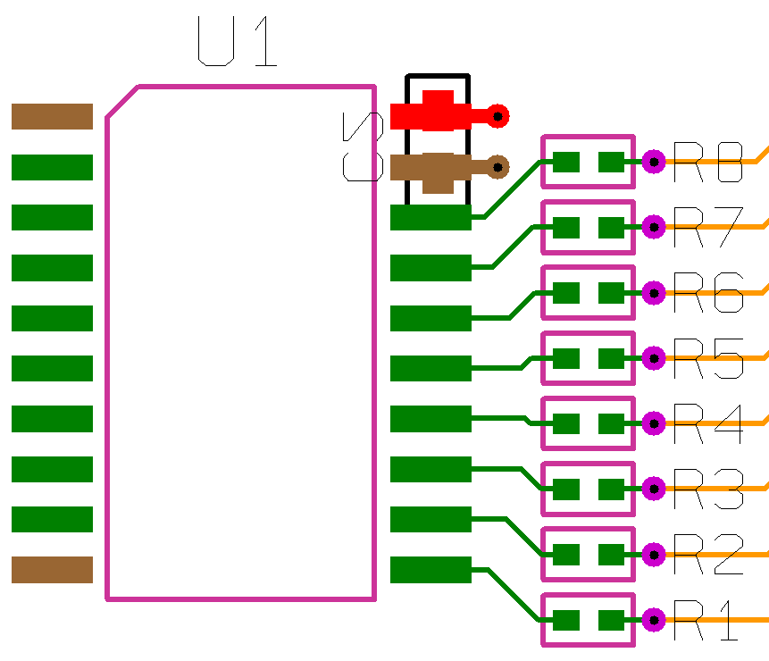
The placement of bypass capacitors is one of the most critical phases of the design process. Failure to place them correctly can completely negate their performance. Also critical is a situation in which there are too few capacitors for particular components. This information should be communicated back to the engineer, whenever it occurs, so that the schematic can be updated.
1. A major factor in determining where to place the bypass capacitors is whether components can be placed on the bottom side of the board.
It is better to place components on the bottom because capacitors can usually be placed under the pads of top-side SMT components. Placing them on the bottom side usually frees up more space for fanout traces and vias. If capacitors must be placed on the top side, they should be located as close as possible to the power pins of the components.
Notice in Figure 1 the bypass capacitor takes up additional space on the top side and therefore reduces the available space for vias. In Figure 2, however, because the capacitor is on the opposite side, we can place it where the pads of the capacitor are directly underneath the pads of the IC on top. This space could not be used for vias, so we have not lost any via space.
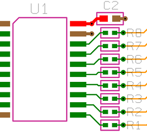
Figure 1: Capacitor on same side
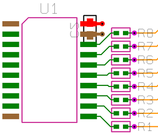
Figure 2: Capacitor on opposite Side
There are differing opinions among engineers regarding how power traces should be routed to the bypass capacitor. Some engineers insist that the trace first connect the device pin to the capacitor and only then go on to the power plane via (Figure 1). Other engineers say, however, that either of the two methods shown in Figure 1 and Figure 2 is more than adequate, and that the placement of the power via with respect to the capacitor land is irrelevant.
An experienced design bureau will use either of these two illustrated methods unless specifically instructed to do otherwise by the engineer. But of the two methods shown, it is preferable to use the one illustrated in Figure 2.
Aside from the benefits of freeing up more via space, this method also has the advantage of keeping the ground path shorter by having the ground side of the capacitor connect directly to one of the device ground pins. This provides a shorter, less inductive ground ‘system’ around the IC. As frequencies increase, this ground loop area is more critical, so it is a good idea to get into the habit for all designs.
2. When multiple capacitors of different values are assigned to the same supply pin on an IC, you should place the lowest value capacitor closest to the device pin.
The lowest value capacitor provides switching current for the highest frequency supply current requirement. When the output of a digital device switches from an ‘off’ state to an ‘on’ state and vice versa, the current required to do this becomes quite high for a very brief period of time. If only large value capacitors are available to provide this near-instantaneous current, then the output will be unable to switch at the required speed due to the longer time constant of these larger capacitors. This can cause serious timing problems in the design. Placing low value capacitors close to the pin helps to supply a small current very quickly to the switching device. This is because of the shorter time constant of these smaller capacitors. Once the output reaches a steady state again, the current requirement is reduced.
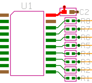
Figure 3: Alternate Routing Capacitors
3. Larger non-polarized capacitors and tantalum capacitors should be placed near the pin or device in ascending order of value. Tantalums are typically used as an ‘area storage tank,’ which provides the required current faster than the system power supply. These tantalums recharge the high frequency capacitors more quickly than the system supply can respond.
In Figure 4 the lowest value capacitor, C13 (10nF 0402), is placed closest to the device power pin, followed by C2 (100nF 0603), and finally C14 (10uF 3216). The tantalum can be placed above or below the device without degrading performance, as long as it is close to U1. Usually the space to the left and right of an IC is required either for fanouts or other components that need to be considered before the tantalum. The number of capacitors of each value will usually decrease as the values increase. So there might be four to six ceramic capacitors per tantalum capacitor. Capacitors with values greater than 10uF can usually be dispersed over a larger area.
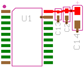
Figure 4: Bypass Capacitors in Ascending Order
5. Devices with multiple power pins usually need to have at least one bypass capacitor per power pin. Looking at the figures below, if the design only allows for two bypass capacitors on U3, then place one on either side of the device, as in Figure 5. However, if this were a 16-bit buffer/driver, it would be particularly susceptible to ground bounce problems, because many outputs can switch simultaneously. If this were the case, then you should make every effort to persuade the engineer to add two more capacitors per device, as shown in Figure 6.
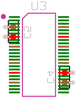
Figure 5: Too Few Bypass Capacitors
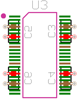
Figure 6: Preferred Number of Bypass Capacitors
6. Always refer to the schematic when placing bypass capacitors because there are often logic input pins on digital devices that are ‘tied high’. Make sure when placing the bypass capacitors that you are placing them at the device power pins and not at tied high logic pins.


![Download Optimum's Designer Handbook! [PDF format]](https://no-cache.hubspot.com/cta/default/317720/240d1413-c945-4cb8-a546-a84937b16039.png)