10.07.2014
How to Bypass BGA Packages

Knowing how to place a bypass capacitor is a crucial step in PCB design. In most cases, we recommend that the bypass capacitor is placed on the bottom side for ideal proximity to an SMT, all while utilizing extra space. But bypassing BGAs can be slightly trickier. BGAs are high desity components with high pin counts, and it's generally harder to acheive the desired proximity.
There are a number of effective methods of bypassing BGA packages, of which the preferred method(s) would vary, depending on the particular BGA pin configuration.
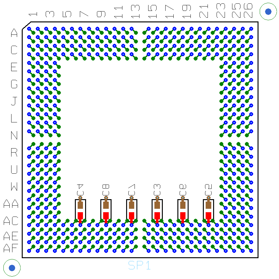
The first method, shown in Figure 12, is for a perimeter matrix BGA. This type of package has pins in rows around a vacant center courtyard. It's quite normal for the power and ground pins of these devices to be on the inside rows. This makes it easy to place the bypass capacitors on the opposite side of the board in the courtyard area. Orient the capacitors in such a way that the BGA power pin fanout via can also be the connection point for the capacitor. This gives the lowest inductance path for power and also leaves via space for signal routing.

Figure 12: Bypass Capacitors in perimeter around BGA courtyard.
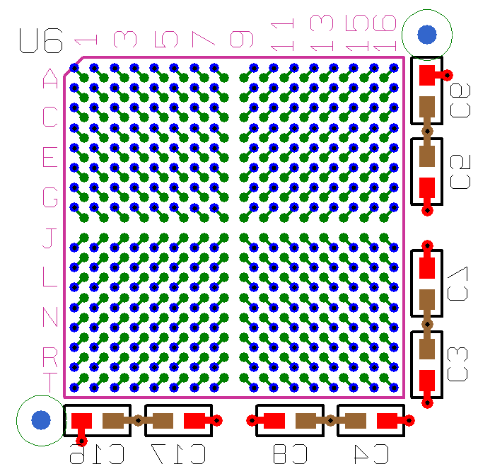
With solid matrix BGA packages as shown in Figure 13 and Figure 14 the bypass capacitors still need to be as close to the device as possible. They can’t be close if they are on the top side of the board because there is usually a 0.200-inch component keepout area around a BGA for rework and inspection tools.

Figure 13: Solid Matrix BGA bypassing (1)
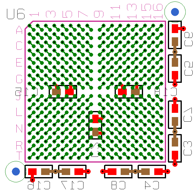
In order to have them close to the device power pins, they need to be placed on the bottom. Placing some capacitors within the matrix as in Figure 14 is preferred, if possible. But this has a disadvantage: the capacitor pads will show up in an X-ray inspection of the board, in which case this method might not be possible. Alternately, sharing vias is acceptable as long as you don’t increase the capacitor trace length to do so.

When placing the bypass capacitors within the matrix, as shown in Figure 14, try to do so only when there are existing vias available as part of the BGA fanout pattern. Adding extra vias in these areas is possible. But be aware that extra vias will reduce the wider channels of copper on the internal power and ground planes that are in these areas as a result of the fanout pattern being in four directions.
Capacitors placed as in Figure 14 often require separate vias for all the connections to power and ground planes. This is usually more of a personal requirement from an engineer. Generally, the more high speed a design is the more this becomes relevant. Sharing vias is often allowed, as in Figure 12, and saves routing channels.
These are only general guidelines for bypassing BGA packages. Often you will find that the engineer has a very specific pattern of bypass capacitors that he or she wants to implement for a particular BGA device.
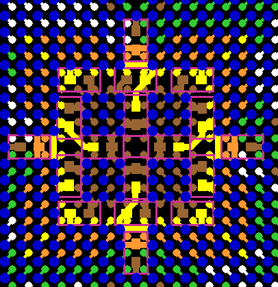
The example in Figure 15 shows eighteen bypass capacitors tightly placed and routed in the middle of a solid matrix BGA.


![Download Optimum's Designer Handbook! [PDF format]](https://no-cache.hubspot.com/cta/default/317720/240d1413-c945-4cb8-a546-a84937b16039.png)