31.03.2014
Lean NPI at ODA Part One: Where Are We Now?
For more than twenty years, Optimum Design Associates (Optimum) has offered their customers PCB design and layout services, and also bare-board assembly. Optimum has customers in many application areas in the electronics industry and specialize in very complex PCB designs. To stay at the top of the competitive heap, they employ advanced design techniques and software solutions to ensure the highest quality possible and avoid costly re-spins due to any factor – design errors, data errors, manufacturability problems, signal and power integrity issues, and a host of other potential issues.
Optimum Design Associates designs printed circuit boards following a standardized design flow, ensuring that the requirements of the customers are met, quality levels are high, and the resulting designs are suitable for PCB fabrication, assembly, and test.
PCB DESIGN PROCESS
Although Optimum has several PCB design tools available, depending on customer compatibility and fabricator requirements, they have used Mentor Graphics tools since the business was founded in 1991. Currently, they employ Mentor Graphics Expedition Enterprise and PADS. With Expedition, they also have Xtreme technology that allows multiple designers to work on the same PCB at the same time.
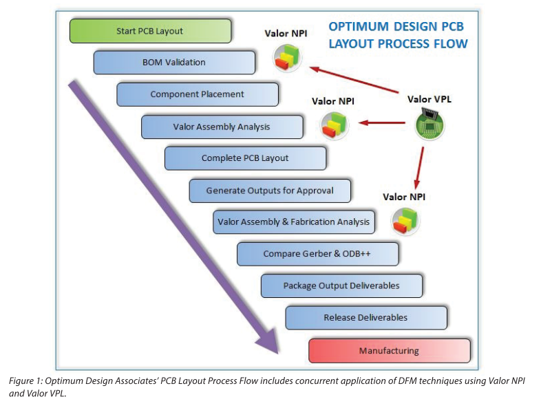
The PCB layout process flow used at Optimum is shown in Figure 1. When the PCB layout begins, the first step is to validate the Bill of Materials (BOM) using Mentor Graphics Valor NPI and Valor Parts Library (VPL). This ensures that all the part-numbers, reference designators and quantities are correct and that VPL package models are available for later use in the design flow. Any missing VPL package models can be generated at this early stage. Once the component placement is completed, the design is subject to Design for Manufacturability (DFM) verification using Valor NPI and VPL.

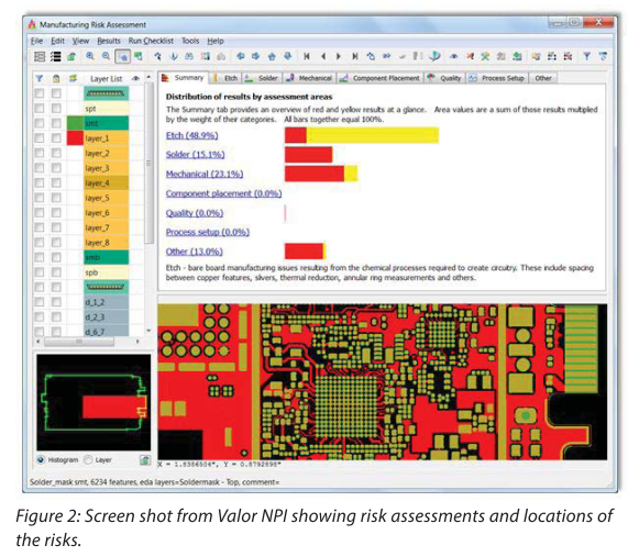
Valor NPI provides comprehensive DFM analysis for PCB fabrication, assembly and test. DFM analysis can be run at any time during the PCB layout process and will report issues which could cause critical problems during manufacture. Without DFM, there may be high levels of scrap or rework, or time-consuming delays during the New Producing Introduction (NPI) process. Figure 2 is a screen shot from Valor NPI showing a DFM summary.
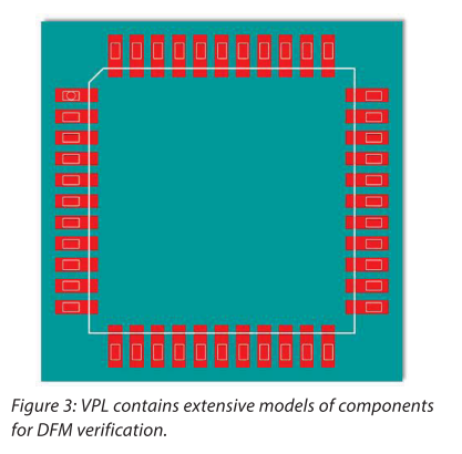
VPL is a dedicated library of electronic component models used in PCB assembly DFM verification. Each VPL package model represents the precise component bodies and pin contact areas for a given manufacturer’s part number, as seen in Figure 3. Using the combination of Valor NPI and VPL, a powerful and comprehensive Design for Assembly (DFA) analysis can be performed. The analysis covers all aspects of PCB assembly and can be considered a “virtual prototype.” Potential solder-joint problems are highlighted using pin-to-pad analysis, and component analysis will catch positional and process related issues during pick-and-place. Any reported issues can be acted upon at an early stage in the PCB design flow.
Following the initial assembly analysis, the design can then be routed and copper planes created. On completion of the layout, provisional outputs are generated and delivered to the customer for design approval. In parallel, a comprehensive fabrication and assembly DFM analysis is performed using the Valor NPI and VPL tools. The analysis results are used to confirm that there will be no quality or process issues during fabrication and assembly of the product. In addition, Valor NPI ensures that the design will achieve the highest possible yields during manufacture. A drop in yield causes increased manufacturing cost due to material waste or repeated processes and increased production time. For both Optimum and their customers, this means real savings in time and money.
DFM BENEFITIS
Some companies still do not employ DFM in the early stages. Instead, DFM is performed at the PCB fabrication vendor, primarily to ensure acceptable yields of bare boards. If significant problems are found, the project must go back to design for a re-layout and then back to the fabricator. This can take days or weeks and incur a hefty cost.
On the other hand, Optimum Design Associates has embraced the concept of concurrent DFM within their PCB layout process-flow. By moving the DFM as early in the product design as possible – “left shifting” it on the product development timeline – running partial checks on available data, problems are relatively easy to correct and cost very little in either time or money. At key stages of the design, Valor NPI examines the PCB layout at multiple points in the design process to assess the viability of both fabrication and assembly, which ensures the design meets the capabilities and process constraints of the manufacturer. The designer takes control of the decision-making process regarding DFM issues so that when it comes to manufacturing handoff the supplier does not need to make changes to the output data.
The last step in the PCB design phase is compiling the electronic files to deliver to the PCB fabricator. Optimum produces a high-quality ODB++ output file as well as the older Gerber-based file sets. Optimum Design Associates offers in-house PCB design and assembly. Optimum can also arrange and manage PCB fabrication with suppliers who prefer to work with ODB++ data.
To ensure consistency between the DFM verified ODB++ data and the traditional Gerber and Excellon drill outputs, Optimum conducts a graphical comparison. Using Valor NPI’s CAM Compare tool, the Gerber data and ODB++ data is overlaid. Layer by layer the data is automatically compared and any differences are reported. Optimum would prefer to use the more intelligent ODB++ format for all customers, but until it is universally accepted, they will deliver both ODB++ and Gerber.
Once it has been established that both types of output format (ODB++ and Gerber) are graphically identical, the final deliverable data can be packaged and released to the customer and the PCB fabricator.
GERBER SHORTCOMINGS
The disadvantages of using Gerber data are shown in Figure 4. Illustrated here is the flow of traditional data, using Gerber format, from the CAD system through to manufacture. Although the traditional data is sent for manufacture, it is not suitable to directly drive the production process and machines. Much effort is required to re-engineer the data, re-introduce the design intelligence and rebuild the product model definition. Once this has been completed, the data can be verified as suitable for the manufacturing processes. Only then can the data preparation and tooling operations be performed and production can begin.
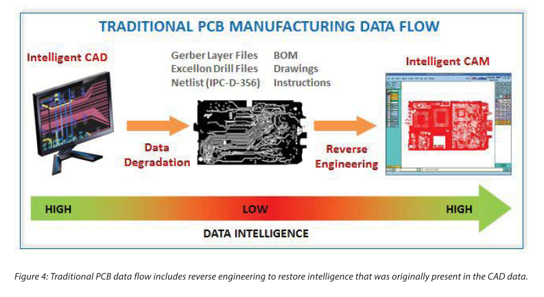
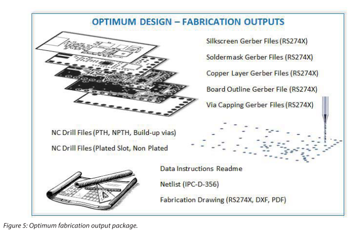
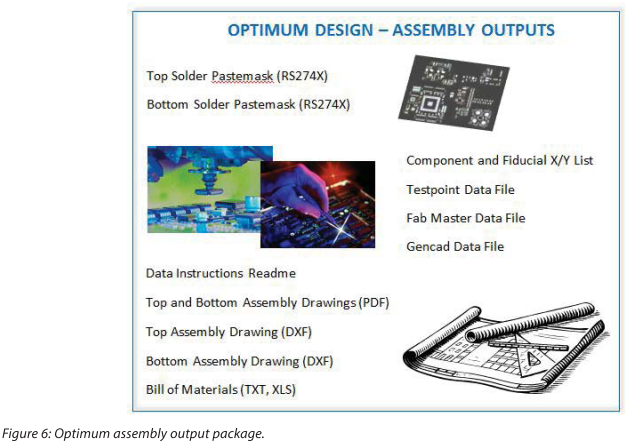
It is clear that re-engineering the product model definition is time-consuming and may result in in misinterpretation of the original design intent. Further to this, different vendors may interpret the product model definition in different ways so there is no guarantee that an identical product will be manufactured by multiple suppliers. In addition to producing data packages for PCB fabrication (Figure 5), Optimum also produces PCB assembly (Figure 6) data packages.
ODB++ IMPLEMENTAION
To alleviate the issues currently associated with traditional data formats for manufacture, Optimum Design Associates’ preferred data type is ODB++. ODB++ is an intelligent data structure that carries all the information required for the manufacture of PCB assemblies. The format was developed over more than 15 years by Valor and is now maintained and developed by Mentor Graphics following the acquisition of Valor.
ODB++ is an open database format and its specification is available to partners of the ODB++ Solutions Alliance. It is universally accepted as the best format for the design-to-manufacture handoff and Figure 7 shows its content.
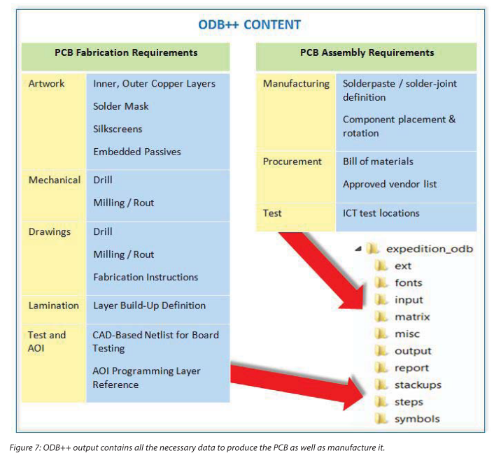
It can be seen that the ODB++ database contains all the same data as the traditional formats but is held within a folder structure which can be compressed into a single file. The data itself carries additional intelligence such as feature attributes. These attributes are compatible with PCB front-end tooling systems and provide a more complete dataset for product model definition. ODB++ can be read directly into the front-end system without the need for any conversion or further preparation or manipulation. Using ODB++ makes the production tooling process much quicker, more accurate, and error-free when compared to using traditional data.
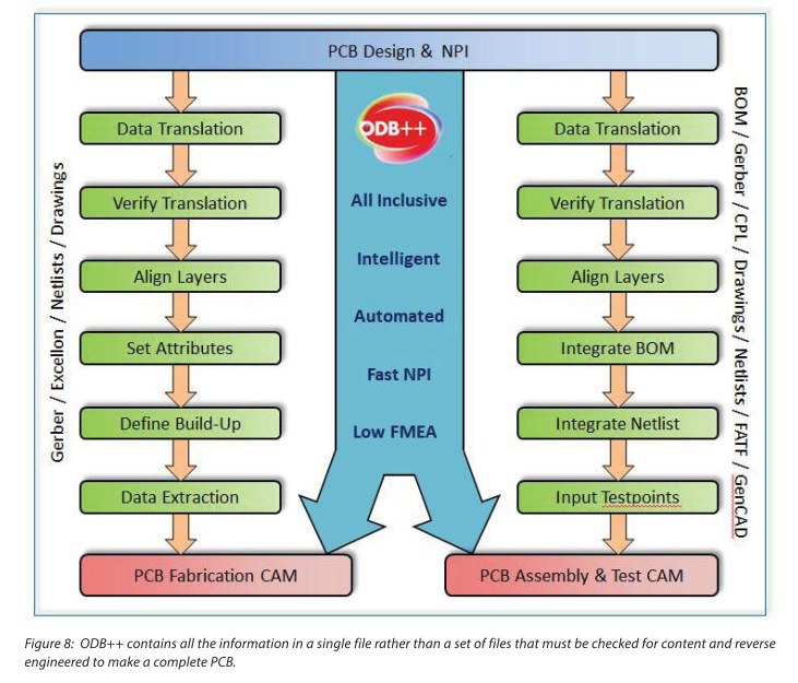
Figure 8 details the differences at the manufacturing front-end stage between using ODB++ and the traditional data formats.
LEAN NPI – THE WAY FORWARD
The Optimum Design Associates vision is to offer their customers a service following the “Lean New Product Introduction (NPI)” product development model. Lean NPI combines concurrent DFM analysis using vendor-supplied rule sets during the PCB layout process and the adoption of intelligent ODB++ as the manufacturing output for handoff to fabrication and assembly. This Lean NPI journey will be implemented as a joint venture between Optimum Design Associates and Mentor Graphics.
The first step will be to replace the traditional manufacturing data formats with ODB++ output as the only dataset for production handoff. Optimum delivers a faster and higher-quality PCB design and manufacturing service using ODB++ as the main dataflow out to manufacturing.
With guidance from their manufacturing vendors, Optimum can move to the next step in their journey. Adding the required attributes and intelligence to the ODB++ data will provide a smooth and direct transfer into the CAM tooling environment.
Optimum has already begun their Lean NPI journey by employing concurrent DFM during the PCB layout flow. As seen earlier, running DFM at key stages in the design saves time and effort during the NPI process. In the final step of Lean NPI adoption, working closely with the manufacturing vendors and running DFM based on their rules will improve quality and yields.
The Lean NPI process will provide a number of benefits to Optimum, including reduced time to manufacture, increased quality, and easier management of data packaging and handling. Optimum Design Associates customers will enjoy those same benefits plus improved product reliability and production repeatability.
In Part 2, we will look at the NPI Process used by Optimum and discuss the stages involved to achieve best-practice Lean NPI.


![Download Optimum's Designer Handbook! [PDF format]](https://no-cache.hubspot.com/cta/default/317720/240d1413-c945-4cb8-a546-a84937b16039.png)