19.12.2014
PCB Library Management Part Five: Miscellaneous Modifiers


Throughout this series we’ve taken a look at almost every facet of library organization, with the end goal of streamlining the process of part identification for library users. Overall library hierarchies, footprint and symbol naming, and pad & Padstack naming have all been covered. A small number of modifiers and special components such as fiducials and mounting holes remain. For the final installment of the library organization series, we'll take a look at fiducials, mounting holes, and other miscellaneous modifiers to the library.
Fiducials
The Optimum library segments Fiducials into two separate partitions. FID_CELL fiducials to be placed locally with cells, and FID_GLOBAL for fiducials placed on the PCB. The parameters for these are as follows.
FID_CELL_0750 = 0.750mm pad, with 2.250mm soldermask opening.
FID_CELL_1000 = 1.000mm pad, with 2.500mm soldermask opening.
FID_GLOBAL = 1.000mm pad, with 2.400mm soldermask opening.
These may be modified or used as is. The default soldermask opening sizes are show above but alternate soldermask opening sizes or other modifications can be added with further _suffix modifiers
Note: Global fiducials are defined with paste mask the same size as the pad to allow for the solder stencil alignment.
Modifiers
There are many options for both Pads and Padstacks that would make full naming very complex and result in excessively long names. The library uses modifiers at the end of names to define any deviations from default values. Modifiers always appear at the end of the names and there may be multiple modifiers, (separated by underscore characters), present in the name. Modifiers are used to define soldermask, solderpaste, via properties, usage type and other miscellaneous padstack conditions. Some modifiers have optional parameters used to specify entity sizes in one or both axes.
The following tables list the modifiers and options used to customize pads or padstacks. When multiple modifier are required for the same padstack the order of modifiers after the padstack base name should be Top – Internal – Bottom – Solder Mask – Solder Paste – Miscellaneous.
Note that not all modifiers outlined herein are currently used in Optimum’s library. There are many that are included for future use.
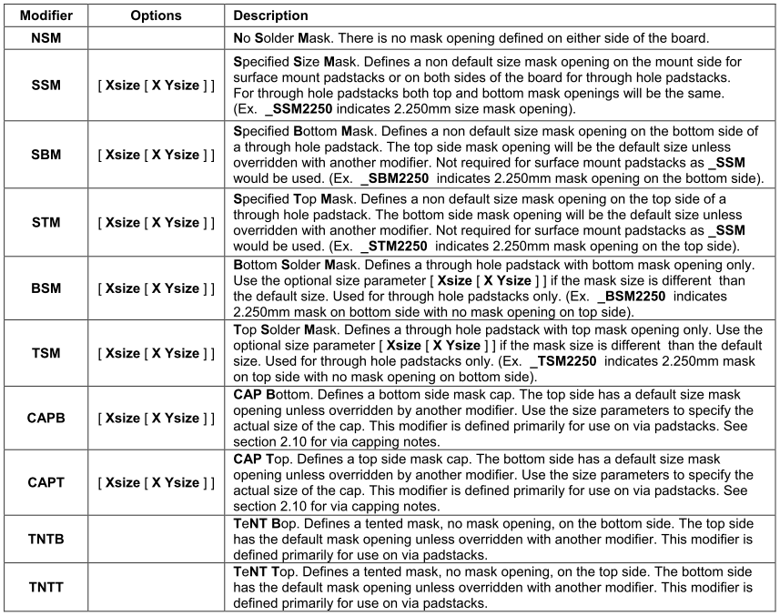
Soldermask Modifiers
Solder Paste Modifiers

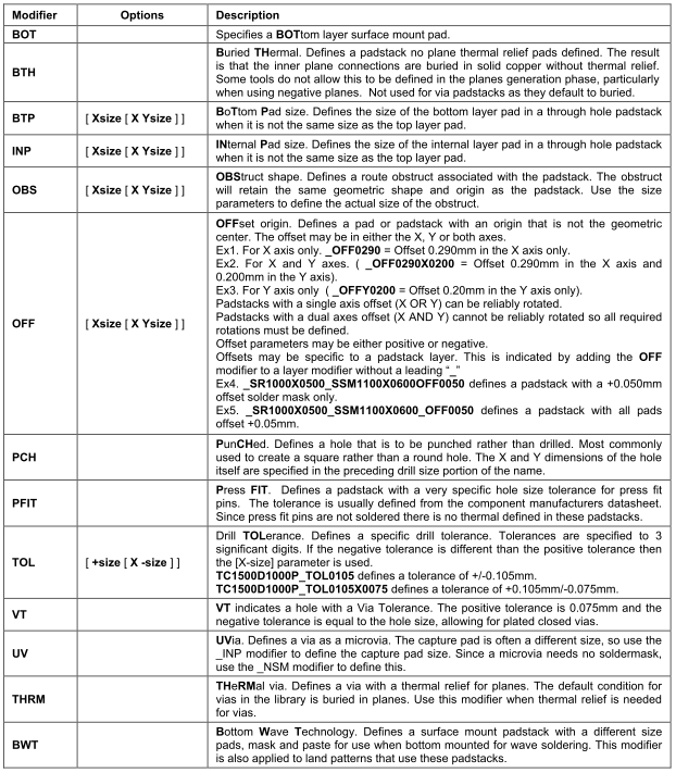
Misc. Padstack Modifiers
Mounting Hole Naming Convention
The naming convention for mounting holes lists the Plating type first, followed by the hole dimensions, the pad shape, and the pad dimensions as follows:
MH [P/N] Xsize [ X Ysize ]] PadShape Xsize [ X Ysize ]
Examples:
MHP300C4000 defines a 3.00mm diameter Plated hole with a 4.000mm diameter circular pad.
MHP250S3800 defines a 2.50mm diameter Plated hole with a 3.800mm square pad.
MHP150X075B2250X1250 defines a 1.50mm X 0.75mm Plated slot with a 2.250mm X 1.250mm obround pad.
MHN300 defines a 3.00mm diameter Non-plated hole. (pad sized according to the table in figure 6.11).
MHN495X445 defines a 4.95mm X 4.45mm Non-plated slot. (pad sized according to the table in figure 6.11).
Note: The only pad shapes used for Non plated holes are octaGon and elonGated octagon.
Non-Plated Mounting Hole
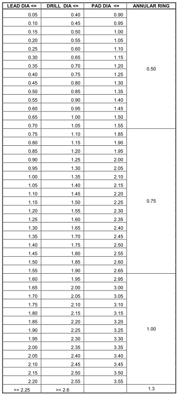
The following table outlines the default pad size per drill size range for non plated mounting holes:

An octagonal pad is used to indicate a non plated hole, or an Elongated Octagonal pad for a non plated slot. For non plated slotted holes the dimensions of the elongated octagon pad are determined in X and Y axes by the range in table above, that the slot dimension in that axis falls within.
A route obstruct is used around non-plated mounting holes to ensure clearance to copper on all pcb layers.
Plated Mounting Hole
The table, Drill dimensions in figure 6.13 outlines the default pad size per drill size range for non plated mounting holes. Pad sizes may often vary from these defaults according to what is required by manufacturer specifications.
If the drill dimensions for a slot through hole falls into different ranges in the table, the annular ring in each axis is based on the range that matches the dimension in that axis.
The clearance to other copper for plated mount holes is controlled in the clearance rules within the layout tool.
Donut Pads
Donut pads are defined with two characters. The first is D to define Donut. The second is the donut shape, either C (Circular) or S (Square). This is followed by two dimensions. The first dimension is the outer diameter of a circular donut or the outer size of a square donut. This is followed by the letters IDC (Circular) or IDS (Square) and a second dimension, which is the internal diameter of a circular donut or the internal size of a square donut. Other modifiers defined in this document can then be applied to the donut as necessary.
Examples:
DC2250IDC1850 defines a circular donut with an outer diameter of 2.250mm and an inner diameter of 1.850mm.
DS2250IDS1850_SSM2400_OFF0500 defines a square donut with an outer size of 2.250mm, an inner size of 1.850mm, a specified solder mask on both top and bottom sides of 2.400mm and the entire padstack is offset by 0.500mm in the X axis.
Via Capping Notes
Via capping is a method of producing what is traditionally known as ‘tented’ or ‘covered’ vias. A fab shop will generally leave all vias unmasked to allow proper cleaning of the board after processing, and then ‘cap’ the vias with a secondary process. This requires separate output files to define the via locations to be capped on the top or bottom of the board. Capping should only be applied on one side of a via to avoid trapped air pockets which can cause blowouts during the assembly process. Capping may be used on both sides of the board but not both sides of the same via. When implementing via capping we suggest using User Draft Layers named User Via Cap Top and User Via Cap Bottom. These layers will need to be added to your Gerber and ODB output configurations to suit your fabrication and assembly processes.
In PADS we suggest using the same layer names, with User Via Cap Top as layer 16 and User Via Cap Bot as layer 17. The use of the cap layers in this manner means that there will be a maximum of 14 copper layers available before switching to Max Layers.
Plane Clearance and Thermals
The plane clearance sizes are based on the drill size. A range of values have been provided based on different ranges of drill sizes in the following table. These values minimize the possibility of overlapping clearance pads on inner planes that can potentially cause a ‘slot’ to develop. Use the plane clearance calculation to determine the default route obstruct when necessary. The route obstruct dimension may be modified at the librarians discretion to allow for pin to pin spacing issues or screw head diameter issues. When an elongated padstack has X and Y dimensions that fall into different ranges in the table, the range that is correct for each dimension should be used. For example, a padstack of THP270X090B3300X1500 is a slotted hole 2.70mm x 0.90mm with an obround pad 3.300mm x 1.500mm. In this case the clearance in the X dimension is 1.000mm over the drill size, but in the Y dimension it is only 0.500mm over the drill.
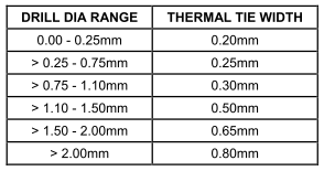
Thermal connection pads are also based on the drill size using the ranges defined in the tables below. When more specific control of the thermal pad parameters is needed there are three modifiers available. See the Thermal Pad Modifiers table for more details about these modifiers.
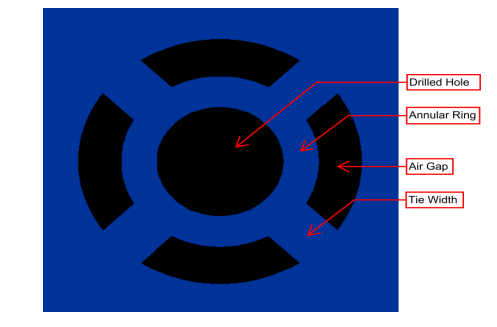
The following tables define the plane clearance and thermal relief parameters for default condition padstacks based on drilled or slotted hole dimensions.

*Thermal air gap is the gap between the inside and outside diameters of the thermal relief.
The tie width is more variable and is shown in the following table. For elongated padstacks, the tie width is chosen based on the range in the table that the smaller of the two hole dimensions falls within.
Thermal Pad Naming Convention
There are two ways to name a thermal pad, drill size based and full detail.
Drill size based naming is simply the shape of the thermal followed by D and then the hole size.
Ex1. TCD125 Defines a circular thermal pad for a 1.25mm drilled hole.
Ex2. TBD125X100 Defines an obround thermal pad for a 1.25mm X 1.00mm slotted hole.
Full detail naming is the shape of the thermal followed by D and then the drill size the same as the drill size based naming method, and then followed by separate specific parameters for the Annular Ring, Air Gap and Tie Width.
Ex1. TCD125A0120G0100T0120 Defines a circular thermal pad for a 1.25mm drilled hole with a 0.120mm annular ring, a 0.100mm air gap and four 0.120mm wide thermal ties at 45 degrees.
Ex2. TBD125X100A0300XG0300T0250 Defines an obround thermal pad for a 1.25mm X 1.00mm slotted hole with a 0.300mm annular ring, a 0.300mm air gap and four 0.250mm thermal ties at 45 degrees.
Thermal Pad Modifiers
The following modifiers are available to provide a more detailed definition of a thermal pad when the default hole size based thermals are not suitable.

Drill Dimensions
Drill diameters are rounded up to the nearest 0.05mm. This table shows the drill size used based on the lead diameter when the hole size is not defined by the manufacturer.
Press fit pins do not follow this rule, they are defined with the size and tolerance specified in the manufacturer data sheet.
The minimum annular ring and pad size for each drill diameter is also referenced. The annular ring may be reduced at the librarian’s discretion if the pin to pin spacing is an issue.
