22.01.2015
Mentor Expedition Library Tutorial: Display Control Settings for PCB Library


Mentor’s Display Control gives designers and librarians myriad options for influencing how a design is displayed on the screen. The goal of any display scheme is to have any information a designer needs readily visible, so more time is spent working, as opposed to scouring the design for the portion you wish to work on. While the individual colors chosen are personal preference, best practices exist for both library and PCB design work. Let’s take a look at how many of Optimum’s librarians configure their Display Controls.
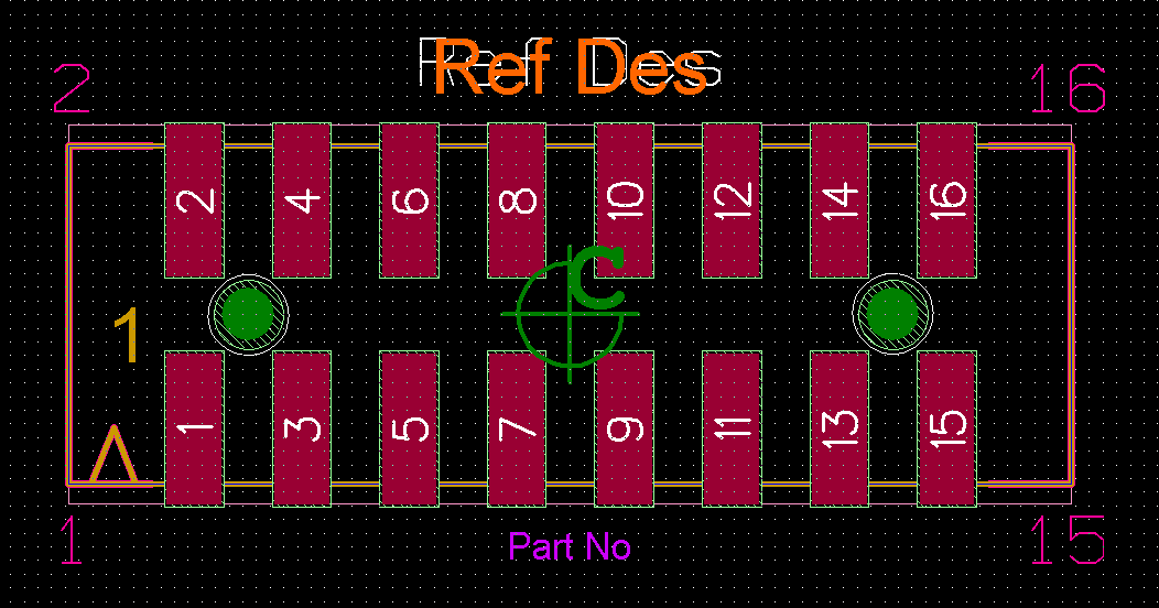
Colors
The goal of adjusting the default colors in Display Control is to ensure all portions of a PCB footprint are visually distinct, and able to be quickly identified by a librarian or designer. Display colors can be adjusted from Mentor Cell Editor by clicking View > Display Control.
Note: For the purposes of this article we’ll be looking at one ODA librarian’s standard setup, individual color choices will vary by user. The most important factor is that all colors be unique for easy identification.
Placement Outline: Dark Blue
Assembly Outline: Yellow
Silkscreen Outline: Dark Pink
DFA Bound Top: Light Pink
Solderpaste Top: Maroon
Soldermask Top: Teal hatched pattern
Solderpaste Bottom: Blue
Soldermask Bottom: Yellow hatched pattern
Mounting Holes: Dark Green
Assembly Part Number: Magenta
Assembly Reference Designator: Orange
Silkscreen Reference Designator: White
Line Widths
Next, we’ll take a look at line and typeface width, height, and font. Maintaining consistency in the library begins with part labeling. Ensuring that labeling is consistent across all parts leads to cleaner designs and less problems during layout and assembly.
The primary goal of line widths for the various part layers in a PCB library component is to ensure that all layers are easily visible when stacked on top of one another. This allows a librarian to quickly verify that all necessary layers for the part are both present, and accurate.
Placement Outline
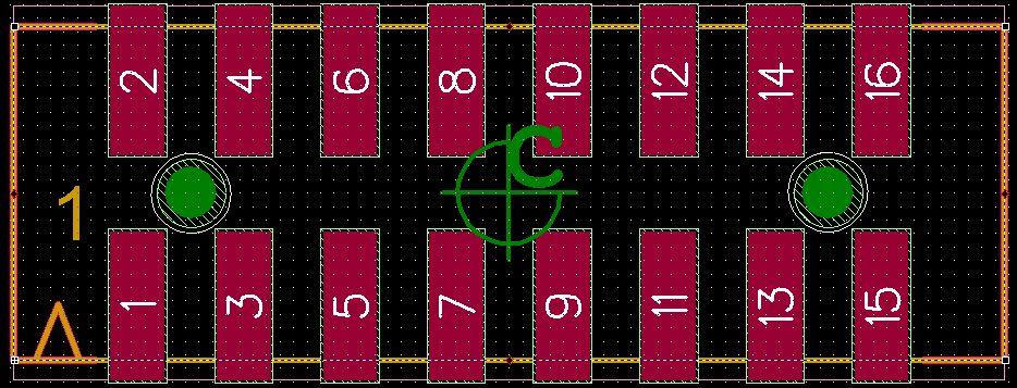
Line Width: 0
Assembly Outline
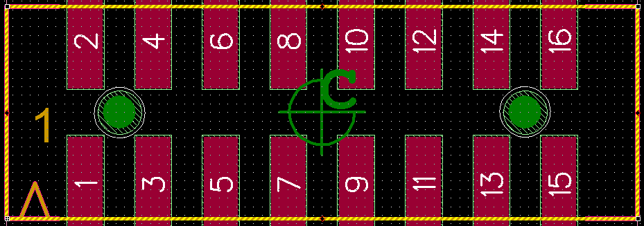
Line Width: 0.1
Silkscreen Outline
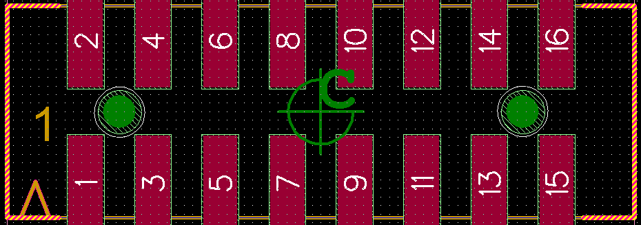
Line Width: 0.12
DFA Bound Top
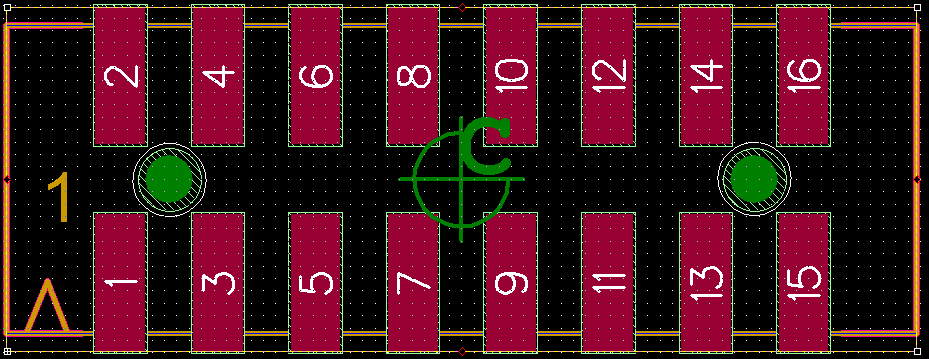
Line Width: 0
Text
The goal of text on a PCB component should be to clearly identify the part number and reference designator to the designer, and have consistent silkscreen sizing for easier assembly.
Assembly Layer Text
Reference Designator

Text Height: 1
Pen Width: 0.1
Font: Arial
Pin 1 Label

Text Height: 1
Pen Width: 0.1
Font: Arial
Part Number

Text Height: 0.5
Pend Width: 0.1
Font: Arial
Silkscreen Layer Text
Reference Designator

Text Height: 0.9
Pen Width: 0.1
Font: Veribest Gerber 0
Pin Number Labeling

Text Height: 0.9
Pen Width: 0.1
Font: Veribest Gerber 0


